PCB 锡测试是测试 PCB 可焊性的一种方案,以评估 PCB 焊盘是否能很好地与锡膏润湿和连接,这直接影响到 SMT 的质量和可靠性。
PCB tin test is to test the PCB solderability of a programme to assess whether the PCB pad can be good with the solder paste wetting and connection, which directly affects the SMT quality and reliability.
Principle of tin test
Printed tin experiment is to unpacked PCB bare board using the corresponding SMT steel plate normal printing paste, directly after the reflow to observe the effect of pad paste wetting to determine the performance of the PCB pad soldering. Even if there is no component mounted, the printed tin experiment can simulate the temperature change and chemical reaction in the SMT process, thus reflecting the quality and stability of the PCB surface treatment.
Advantages and disadvantages of printed tin test
The advantages of printed tin experiment is:
It can verify whether the steel plate opening design is appropriate and whether the PCB surface treatment is good.
By comparing different types or batches of PCBs, potential problems or differences can be identified and timely improvement measures can be taken.
It can be used as a means of quickly screening or verifying PCB suppliers, improving procurement efficiency and quality assurance.
The disadvantages of the printed tin experiment are:
The process is more complex and requires preparation of steel plates and solder paste, as well as reflow equipment.
The cost of equipment and materials is high, and it takes up space and time.
The results are affected by a variety of factors, such as steel plate cleanliness, solder paste quality, reflow temperature profile, etc. Therefore, it is necessary to strictly control the process parameters and conduct sufficient data analysis and comparison.
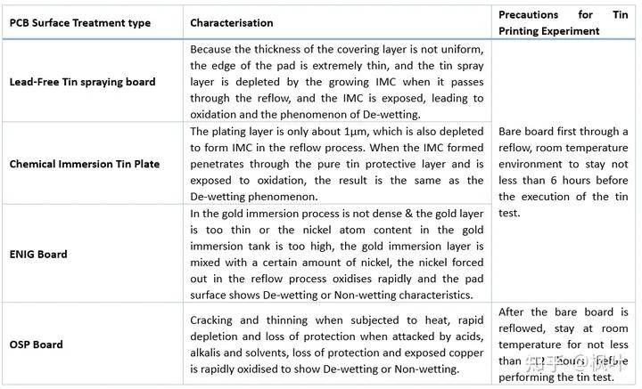
Different PCB surface treatment characteristics
Different PCB surface treatment characteristics have different effects on the results of tin printing experiments. The following are several common PCB surface treatment types and their characteristics:

Tin-on-tin test conditions and results
The conditions and results of the tin-on-tin test need to follow the relevant standards or specifications. The following are the general tin test conditions and results:
Experimental conditions:J-STD-003C-2014, IEC68-2-69, QJ831B-3.7.6.1/3.7.6.2; Newly opened PCB + normal production using reflow parameter settings + room temperature environment.
Experimental results:Solder paste melted area / solder paste printing area > 95%; solder paste wetting range shall not appear De-wetting or local refusal to solder, back wetting phenomenon.


 客服
客服


 小程序
小程序


 公众号
公众号

